APU signs semiconductor training agreement with Mimos Technologies
Separate training streams will cover up to seven engineering academics and up to 20 eligible students per intake.
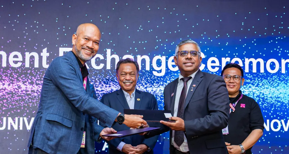
A three-year agreement between Mimos Technologies Sdn Bhd (MTSB) and Asia Pacific University of Technology & Innovation (APU) will give the university’s lecturers and students practical wafer fabrication training in Malaysia. Participants will use equipment and facilities at MTSB’s Semiconductor Technology Centre (STC), with access to its technical expertise.
For lecturers, the programme includes a single professional development course accommodating up to seven engineering academics. It aims to help them align their teaching with fabrication practices. A separate student stream will provide practical fabrication experience for up to 20 eligible students in each intake.
Responsibility for technical teaching, safety procedures and specialist mentoring will sit with MTSB. The university will choose participants and administer their involvement, as well as oversee compliance with requirements covering operations and intellectual property.
The partners signed the memorandum of agreement in Kuala Lumpur at the Mimos Technology Preview 2026. MTSB handles commercialisation for Mimos Berhad, the national centre for applied research and development under Malaysia’s Ministry of Science, Technology and Innovation.
MTSB chief executive Afdzal Syahadat Husni Husin said the partnership aimed to connect academic knowledge with industrial work and develop skilled workers for the country’s wafer fabrication sector.